Plasma-Therm recently acquired OEM-Group and has expanded its Physical Vapor Deposition (PVD) catalog to include the Endeavor systems. This includes the Endeavor MX PVD system.
What is the Endeavor MX PVD?
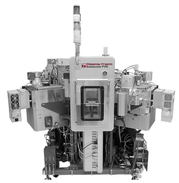
The Endeavor MX PVD is used to deposit thin, conductive films onto wafers 150 mm to 200 mm in diameter. In particular, vias and contact layers can be placed quickly and predictably. PVD processing allows for a dense, uniform coating with very low residual stress, meaning mechanical and electrical properties are consistent throughout. Furthermore, low residual stress means thin films are protected from spallation due to thermal cycling in future processing steps.
The Endeavor MX system uses PVD through sputtering. This means processing can be performed at lower temperatures than PVD through evaporation. Furthermore, due to the high temperatures, an equivalent cooling system is required to dissipate the heat at the completion of the batch run, and to ensure proper deposition. The sputtering process is more energy efficient and safer than evaporation methods.
The Endeavor MX PVD system operates at low temperatures and low pressures, relying on sputtering as a means of depositing the films. A dual-cathode S-gunTM magnetron blasts the sputtering target, dislodging and vaporizing atoms that will be used in the coating. These dispersed atoms, still in the vapor state, travel through the chamber, depositing on the surface of the wafer and condensing into a dense, solid coating.
Why use the Endeavor MX PVD?
Highly oriented AlN films without heating and biasing
The Endeavor MX system can deposit exotic materials, such as Aluminum Nitride (AlN) or Scandium-doped Aluminum Nitride (ScAlN). The challenge with these two materials is that the coatings must be dense and of a specific crystallographic orientation, all of which is made possible through the Endeavor system. Furthermore, the system does not require additional heating or potential biases to ensure the deposition, meaning a reduced chance of damaged dies.
High quality ScAlN deposition
ScAlN films must be deposited in a dense, uniform layer to ensure minimal variation from die to die. The Endeavor MX system allows for tight control of process parameters to guarantee this specialized coating.
Full-face deposition
PVD processing coats the entire surface of the wafer during one batch operation. This means coatings can be deposited much more quickly than other methods, which require a rastering and scanning routine of each die on the surface of the wafer.
6 process module capability
With six process modules, the Endeavor MX PVD system is versatile and ready for several different operations. This increases throughput and reduces tool changing time.
Simple size conversion from 150mm to 200mm
When a tool change is required, such as changing between wafer sizes, the Endeavor MX PVD saves time and effort. Changing handling tools to service 150 mm to 200 mm wafers and vice-versa can be performed quickly and easily.
Independent stress control
With many process parameters under engineering control, inherent stress due to the coating process is minimized. These parameters can be adjusted for each material that must be deposited.
Pt, Au, Ir, Pd and Ru electrode etch
The MX system has a high density plasma source that can be used for etching metals and piezoelectric materials, such as lead zirconia titanate (PZT). To control the etch, the engineer has individual control over the ion density and the ion energy.
High selectivity etch for PZT stopping on Pt
PZT can be etched away selectively, stopping at platinum contacts and vias. This is a major advantage over wet etching and some dry etching techniques, which would attack the platinum as well.
Unaffected by sensitivity to conductive metal deposits
In some plasma processing equipment, conductive metals can affect the etching process. The Endeavor MX PVD suffers from no such limitation.
Independent control of ion density and ion energy
To control the etch, the engineer has individual control over the ion density and the ion energy. By fine-tuning these parameters, engineers can customize the etch rate and selectivity of the etch.
Low pressure low temp process capability
Unlike other PVD methods, such as evaporation, the Endeavor MX PVD does not require high temperatures. Processing is performed under vacuum, and the sputtered material is removed without heating.
Enhanced plasma density at low pressure
By processing under vacuum, plasma density is increased, yielding a more uniform coating. The material being deposited is efficiently sputtered away and condenses on the wafer surface.
Which Endeavor Legacy Systems does Plasma-Therm Support?
Endeavor AT PVD
The Endeavor AT can perform Silicon Nitride (SiN) encapsulation, which is used to precisely control the temperature coefficient of resistance (TCR) for resistive films. This means very temperature-stable resistors can be developed on the wafer. It can also be used to provide bump and backside depositions.
Since Plasma-Therm’s acquisition of OEM Group, they have been servicing and supporting the Endeavor AT PVD legacy systems.
Endeavor EUV PVD
The Endeavor EUV PVD system is specifically designed for metallization of reticles used in lithography steps. These reticles form the masks that expose certain parts of the photo-resist covered wafer to the light source. Because each mask contains proprietary information about the final product, it is often advantageous to produce the masks in-house, versus outsourcing them. With the Endeavour EUV, this is possible. Furthermore, for research and development purposes, it can be more cost-effective to produce the masks in-house.
The system will handle a standard 6” x 6” reticle, and is configured in such a way that no direct contact is made with the sensitive front and back sides of the reticle. Using a unique “sputter-up” design, particle contamination is greatly reduced, meaning reticles have more usable mask space and fewer defects to pattern.
Since Plasma-Therm’s acquisition of OEM Group, they have also been servicing and supporting the Endeavor EUV PVD legacy systems.
Final Word
The Endeavor MX PVD system has distinct advantages in semiconductor processing of thin films and plasma etch. It can be used to deposit a number of materials in dense, consistent layers at a specific crystallographic orientation. The sputtering process does not require the use of bias voltages or heating and cooling mechanisms for deposition.
To learn more about the Endeavor MX PVD system, contact Plasma-Therm.