During the processing of nearly all solid-state electronics, there is an etching step utilizing plasma technology. The two most often used approaches are parallel plate reactive ion etching (usually simply referred to as RIE) or inductively coupled plasma reactive ion etching (usually referred to as ICP RIE). However, with the evolution of device performance, the variety of materials has increased along with the increasing demands on the device structure themselves. The interest in these materials and structures has opened up another avenue for plasma etching, ion beam etching (IBE), and reactive ion beam etching (RIBE). This suggests the two questions: what are IBE and RIBE and what are the applications where IBE and RIBE should be considered?
What is Ion Beam Etching Technology?
Ion Beam Etching is a variation on a theme in that the plasma source used to generate ions is an inductively coupled plasma. The primary difference between the traditional RIE and ICP RIE configurations for plasma etching and IBE is that the plasmas in RIE and ICP RIE rely on substrate bias to attract and accelerate the ions whereas in IBE the ions are accelerated remotely. In the figure shown below, one can see the cross-section showing the IBE source which is simply a relatively smaller ICP source. The size of the source is comparable to the largest wafer size expected to be used.
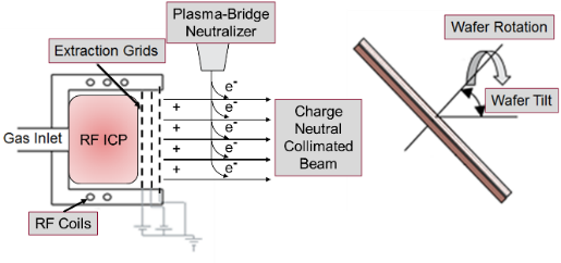
Gas is introduced into the source where a high-density plasma is generated. Argon is the typical gas due to its ease of ionization (one of the lowest values) and its abundance. Helium and xenon can be used to take advantage of their respective lighter and heavier masses but argon is by far the most frequently used. Once the argon atoms have been ionized through the collisions with electrons, they exit the source through a combination of grids that control the acceleration and hence their energy. The grids also serve to collimate the beam towards the substrate and for this reason IBE sources are often called “ion guns”. Since the ions have an energy defined by the grids it is unnecessary to bias the substrate.
Because the ion source is an ICP and the density of ions is greatest in the center, the ion flux is also largest in the center of the beam. This accounts for small amount of nonuniformity in ion flux at the wafer. The plasma-bridge neutralizer is a source of electrons to reduce the ion-ion repulsion that would cause beam spreading. It also avoids charging when insulating substrates are used.
As might be expected, once the ions impact or bombard the substrate, they transfer some of their energy. Upon impact, the ions can eject material much like a billiard ball hitting a rack of balls. The number of atoms removed per ion is the sputter yield and is a function of the material, ion mass and energy, and the incident angle of the ions relative to the substrate. The ability to control the angle of incident ions opens up unique possibilities and applications.
As with most etching technologies, there are variations to achieve specific etching performance in specific applications. One such variation is to add gases to the IBE source that can produce very reactive species such as radicals (atoms or molecular fragments with unpaired valence electrons). This technology is called reactive ion beam etching or RIBE. Depending on the material being etched, the addition of radicals can enhance the sputter yield and hence, the etch rate. This in turn may influence the selectivity between the mask and the material being etched or between materials. The profile of the etched structure might also be improved.
What Applications Use IBE?
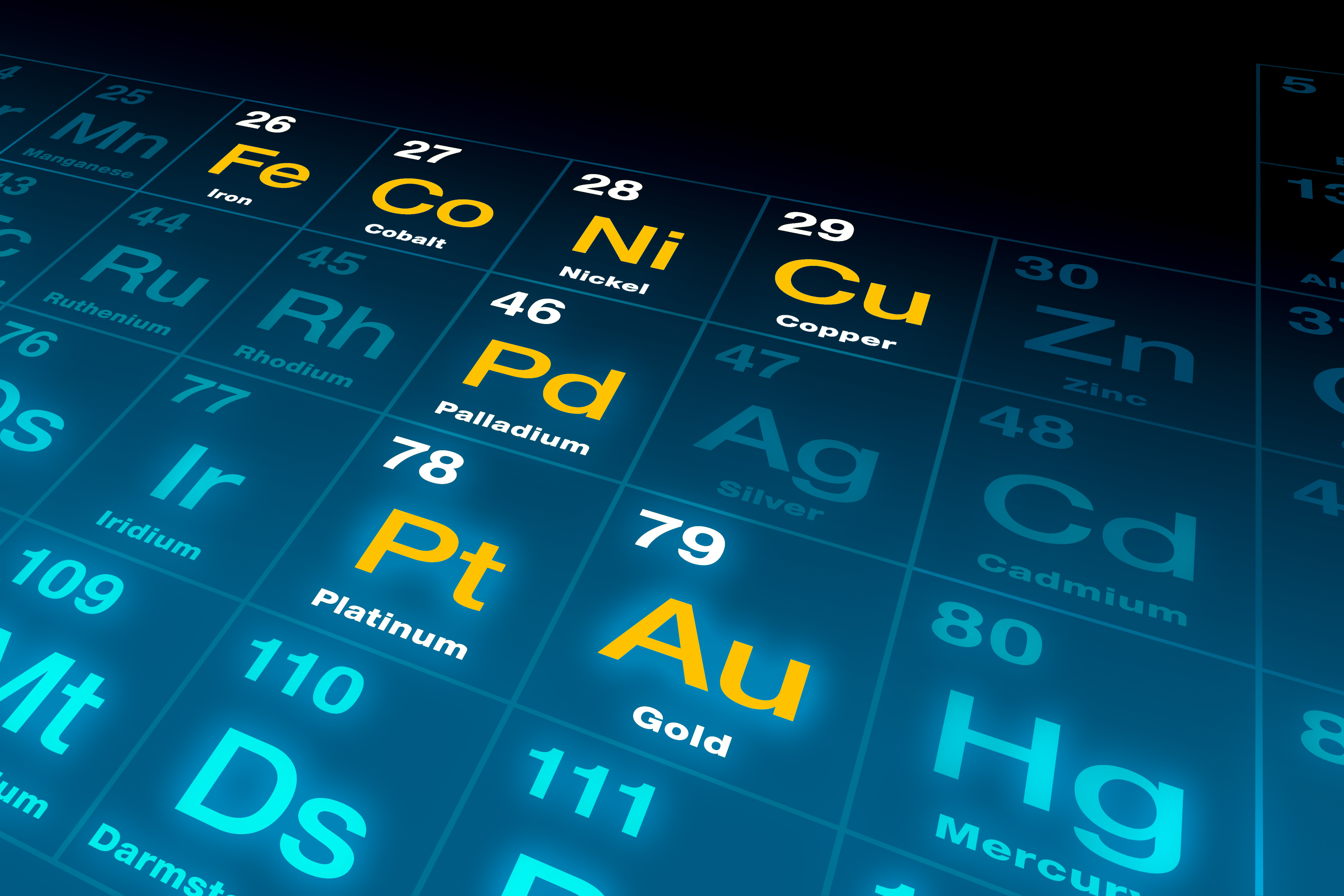
The physical nature of the IBE process, i.e. directing accelerated ions with a controlled energy, suggests applications where the material is difficult to remove by chemically based reactions. Many such materials are now in use in applications ranging from MEMS to RF filters to memory. “Difficult” materials include noble metals such as gold and platinum, piezo electric materials such as PZT (lead zirconate titanate), LNO (lithium niobate), and AlScN (aluminum scandium nitride) used in MEMS and acoustic wave RF filters, or materials used in complicated memory structures such as MRAM and STT-MRAM such as Al2O3, Ni, Fe, Cr, Co, Cu, Mn and Pd to name a few. In addition to being chemically resistant to typical plasma chemistries, the device structures using these materials also need smooth etched surfaces and sidewalls. Material stacks with layers that have different chemical etch rates may end up with an uneven sidewall where some layers have etched laterally more than others. The physical mechanism in IBE leads to much smaller differences in etch rates and contributes to a smoother transition between layers.
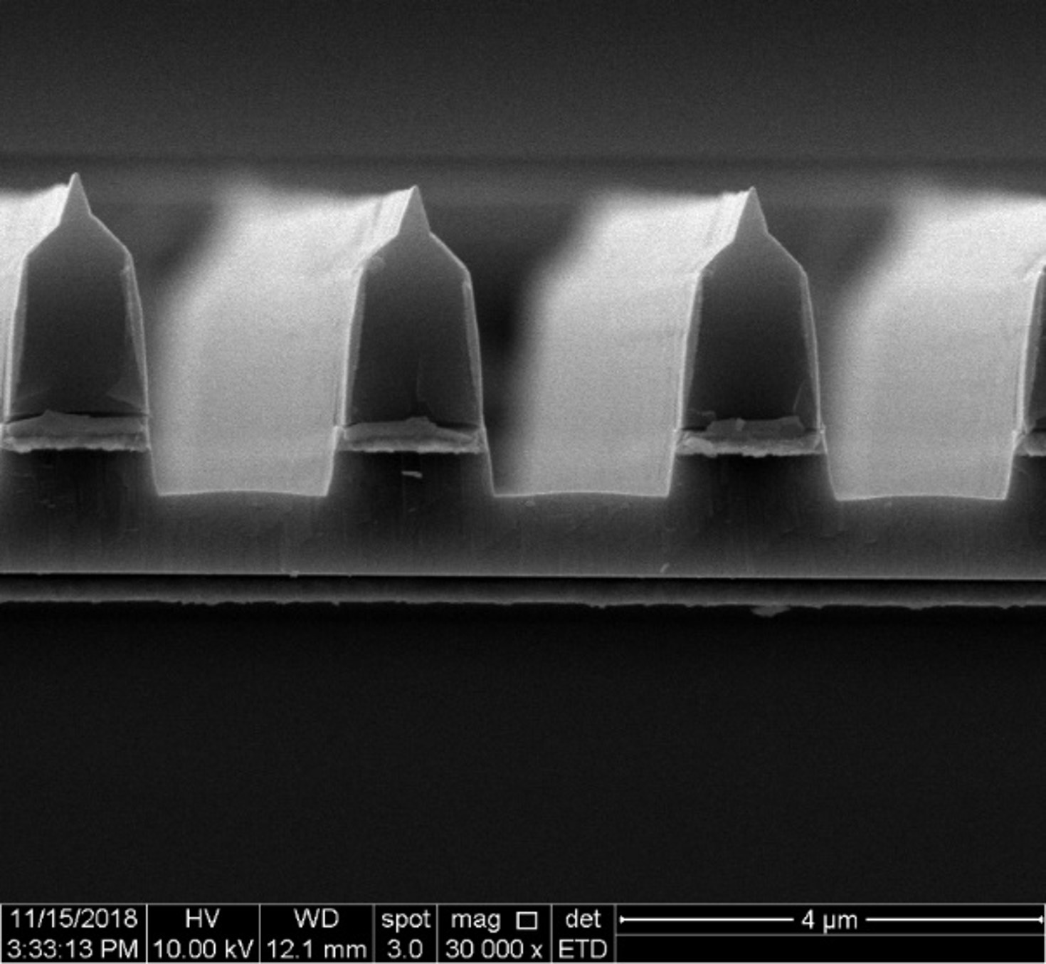
Image: RIBE of ScAlN with CxFy for BAW
However, because the IBE mechanism is based on ejected material rather than evaporated or volatile byproducts, the ejected material is redeposited rather than pumped away. One might ask, then why not simply use ICP RIE and bias the substrate so that the ions do the same thing as the IBE? The answer is the ability to tilt the substrate relative to the ion beam source. This helps remove the material that has been expelled and redeposited on the sidewalls. Depending on the aspect ratio of the structure, the critical feature dimension or profile may be affected. This capability to remove sidewall redeposition is very important to many devices that utilize layered structures. Since sputter yield has angular dependence, there is a preferred angle where the sputter yield is maximum. For some applications this means the etch rate can exceed that of traditional ICP RIE with additional increases in selectivity and profile. The ability to easily tilt the substrate provides an incentive to apply IBE to other applications such as surface smoothing and asymmetrical shapes.
As mentioned above, RIBE utilizes a reactive gas that can add a chemical etching component to the process. For example, fluorine (F) containing gases such as CF4 can be fed into the ion source to create F radicals. In the presence of F radicals there is the possibility of increasing etch rates, selectivity, and profile through ion enhanced etching. The combined effect of radicals and ions has proved beneficial for etching applications the last 40 years.
Summary
IBE and RIBE provide some unique benefits for etching challenging materials and structures. The capability of carefully controlling ion energy for low damage requirement, forming a neutral beam to avoid charging insulating materials, tilting the substrate relative to the ion beam to remove sidewall redeposition, and being able to rotate the sample for high uniformity all contribute to the growing interest in IBE technology.
Check out Plasma-Therm's QuaZar™ Ion Beam Etch and Deposition Systems.